31. July 2023
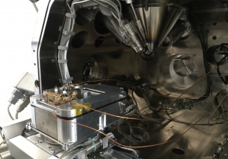
Exploring new materials for chip production and enabling their analysis directly in the production environment – these are the tasks of two scientific teams from #brnoregion – from Thermo Fisher Scientific and Brno University of Technology. Electron microscopes play a key role in their efforts. Thanks to them, as part of the three-year European ALL2GaN project, we can look forward to a solution that has enormous potential to save energy and thus mitigate the climate crisis by reducing CO2 emissions. Indeed, the gallium nitride chips being developed will be used in a wide range of applications including telecommunications and e-mobility.
Chips for solar cells and electric car chargers
Gallium nitride chips provide more energy in a small space and convert energy highly efficiently. As a result, they directly contribute to savings and cutting-edge innovation in green technology. They have the potential to save up to 218 million tonnes of CO2 per year globally in the wide range of applications they will be targeted in the project.
"In the Czech Republic, we are generally quite sceptical about green energy. However, if all the types of chips we are involved in developing in the project are applied, they will save about one-sixth of the world's annual electricity production from nuclear power plants. This is crucial for Thermo Fisher Scientific. Sustainable design is not only a direct technical parameter of our devices, but we are also involved in the development of solutions that contribute significantly to sustainability, as in the case of the All2GaN project," describes Tomáš Vystavěl from the development team of the world's leading electron microscope manufacturer.
Telecommunications, data centres and server farms will benefit from the new generation of GaN chips, as well as e-mobility, renewable energy and highly efficient smart grid solutions."Although gallium nitride has been a long-studied material, there are still many questions and technological challenges that, if solved, will enable the production of advanced chips at an attractive price point. The aim is to use the new knowledge in components that will fundamentally change the power electronics market – more efficient voltage converters, electronics in energy conversion devices such as solar cells, or a powerful wireless charger for electric vehicles are planned," says Miroslav Kolíbal from the Faculty of Mechanical Engineering and CEITEC Brno University of Technology.
Investigating dislocations using electron microscopes
The path to applying these advanced chips to power electronics starts with materials research. "We are involved in the analysis and development of gallium nitride substrates for chip fabrication. The material contains dislocations – line defects in the crystal lattice, which can cause the chip to function differently from how it was designed. We are contributing to enabling chipmakers to work with substrates with a minimum number of dislocations," says Tomas Vystavěl, who describes the involvement of the Thermo Fisher Scientific development team.
Devices that allow resolution down to the atomic level in some cases play a crucial role in chip development. "In Brno, we are developing microscopes that allow us to observe and quantify possible defects in the chip without damaging it, which is a great added value. This so-called non-destructive characterisation is done thanks to unique scanning electron microscope techniques," he explains.
The next phase of the research involves the preparation of a thin sample, which is then observed in a transmission electron microscope and leads, for example, to the discovery of the causes of chip failure. "This is where we work with colleagues from the BUT who are experts in the physics of defects and find out how they can affect device properties," Vystavěl mentions the close connection to Miroslav Kolíbal's research team.
"We will support Thermo Fisher Scientific's research with complementary advanced analytical techniques. In this respect, the infrastructure of the CEITEC Nano Research Centre is key for us," says Miroslav Kolíbal, who is involved in materials physics and nanotechnology and makes extensive use of electron microscopes manufactured in Brno in his research activities in these areas.
"In the project, like Thermo Fisher Scientific, we are focusing on dislocations, which in physicists' terms is a linear disorder in the regular arrangement of atoms in a crystal. One of the research tasks is to observe the movement of dislocations in GaN material using a transmission electron microscope. And in collaboration with other industrial partners, we will be involved in the application of selected analytical techniques in a production environment," summarizes Kolíbal involvement of his team in ALL2GaN.
Renowned experts from Brno
The two Brno teams were not among the 45 project partners from 12 European countries by chance, but they are well established in the semiconductor industry. In the past, experts from Thermo Fisher Scientific have successfully solved projects related to the characterization of crystal lattice defects with manufacturers connected to IMEC in Belgium, for example.
The development of detection techniques for the analysis of surfaces and solids is historically anchored at the Brno University of Technology as well – research group of Professor Tomáš Šikola research group was involved in the successful development of the UHV SEM microscope in cooperation with Tescan, and the research group also gave rise to the spin-off NenoVision. "We have worked specifically with gallium nitride before in cooperation with onsemi, so we have experience in basic research focused on this material," says Miroslav Kolíbal.
The involvement in the All2GaN project thus only confirms the cutting-edge research in the region linking electron microscopy and the semiconductor industry. According to the associate professor from the Institute of Physical Engineering at Faculty of Mechanical Engineering, this can have an even greater impact in the future: "In line with the current activity of the Chips Act, it can help Europe to establish a leading position in power electonics – unlike to logic circuits in processors, a realistic segment of the semiconductor industry."
A significant contribution to this is being made by researchers and companies in the #brnoregion, the location from which the establishment and activities of the National Competence Centre for Chips will be coordinated.
About the project
The project ALL2GaN (Affordable smart GaN IC solutions for greener applications) concerns easy-to-integrate energy-efficient gallium nitride chips. These have the potential to increase energy efficiency by 30 percent in a wide range of applications such as charging mobile devices, powering data centers, voltage converters for homes and on-board chargers for electric vehicles, saving up to 218 million tons of CO2 worldwide. Under the leadership of Infineon Austria, the project brings together a total of 45 partners from 12 countries with a budget of around €60 million between March 2023 and April 2026.


 Share
Share


